Saki – BF-3Si-LS2
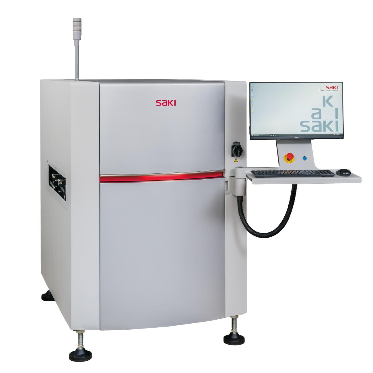
Saki – BF-3Si-LS2
Contact us

Nick Janssen
Product specialist
Description
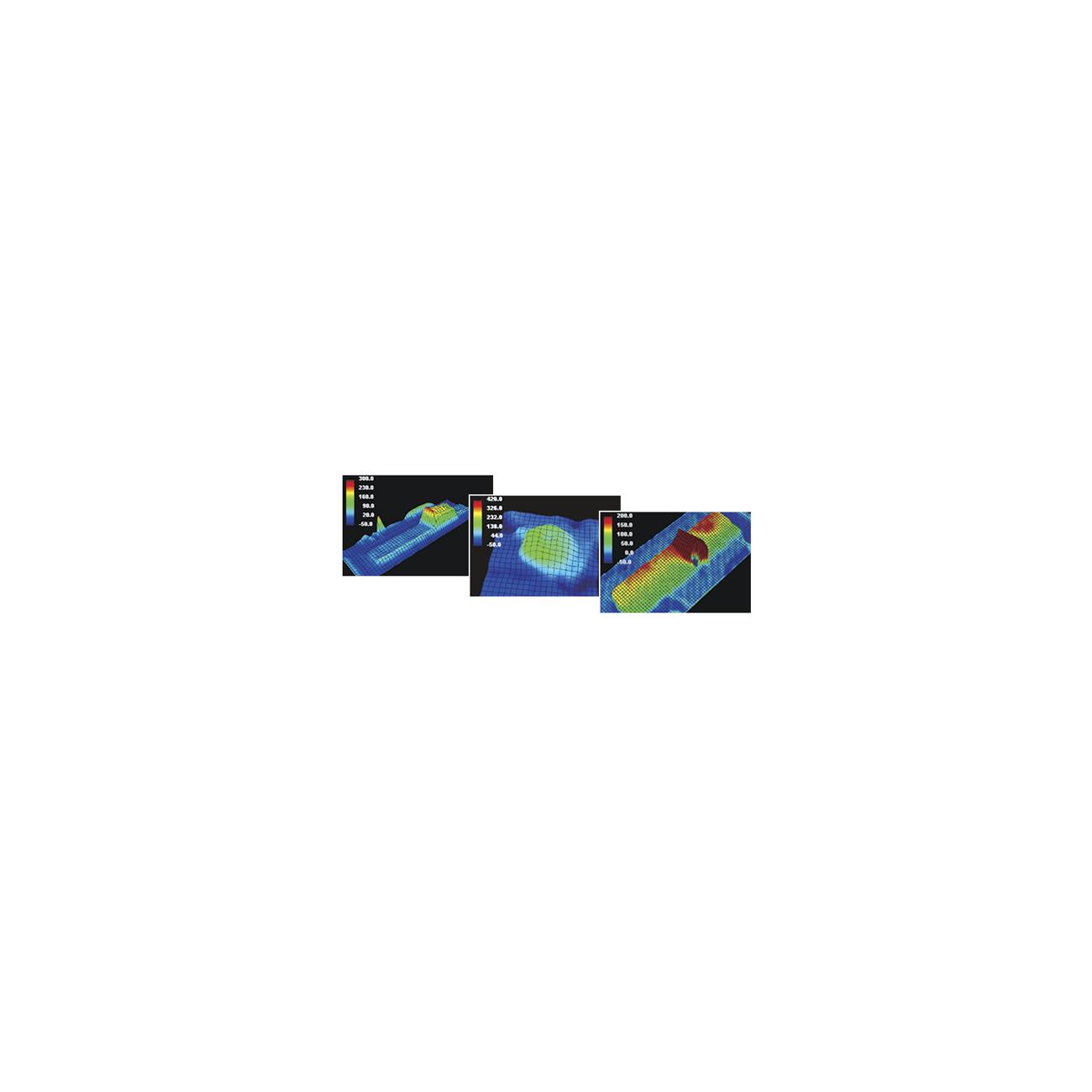
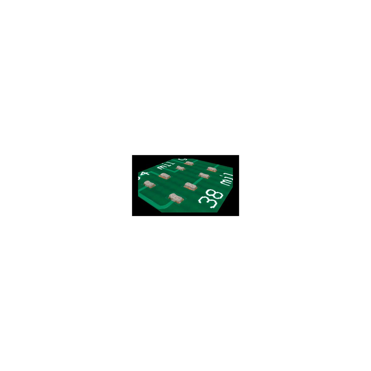
Solder paste is applied during the printing process and is necessary to attach the components to a circuit board to assure the proper electrical connection. The printing process has become extremely complex due to today’s circuit board configurations that pack very small components into extremely tight spaces. Over 50% of circuit board defects are rooted in problems related to solder paste printing. To accurately determine the accuracy of the printing process, 3D solder paste inspection has become a requirement.
Specifications
| Type | |
|---|---|
| Length (mm) | |
| Height (mm) | |
| Weight (kg) | |
| Power | |
| Compressed air | |
| Min. PCB length (mm) | |
| Min. PCB width (mm) | |
| Max. PCB length (mm) | |
| Max. PCB width (mm) | |
| Inline | |
| PCB Clearance Top (mm) | |
| PCB Clearance Bottom (mm) | |
| Resolution camera head (µm) |
Solder paste is applied during the printing process and is necessary to attach the components to a circuit board to assure the proper electrical connection. The printing process has become extremely complex due to today’s circuit board configurations that pack very small components into extremely tight spaces. Over 50% of circuit board defects are rooted in problems related to solder paste printing. To accurately determine the accuracy of the printing process, 3D solder paste inspection has become a requirement.
| Type | |
|---|---|
| Length (mm) | |
| Height (mm) | |
| Weight (kg) | |
| Power | |
| Compressed air | |
| Min. PCB length (mm) | |
| Min. PCB width (mm) | |
| Max. PCB length (mm) | |
| Max. PCB width (mm) | |
| Inline | |
| PCB Clearance Top (mm) | |
| PCB Clearance Bottom (mm) | |
| Resolution camera head (µm) |


