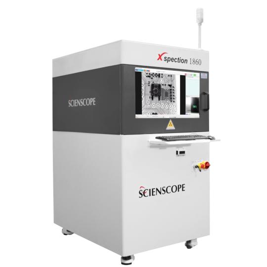
Scienscope - X-ray Inspection System Xspection 1860
IP-fc9147c3
A versatile X-ray machine that offers comprehensive circuit board defect detection and quality assurance for the SMT industry worldwide.
Scienscope - X-ray Inspection System Xspection 1860
IP-fc9147c3
A versatile X-ray machine that offers comprehensive circuit board defect detection and quality assurance for the SMT industry worldwide.
Besoin d'assistance, d'installation et/ou de formation ?
Appelez-nous +32 (0)14 42 44 01 ou contactez nous
Description
With a single closed tube and tilting features, the Xspection 1860 delivers high-resolution imaging perfect for batch inspections. It also provides detailed statistics to help improve your SMT line process. This makes it an excellent tool for inspecting various components, including multilayer PCBs, voids, Barrel Fill (THT), and others.
Features
- Fully integrated 90kV microfocus sealed tube
- Spot size down to 5µm
- Mapping camera tor close-up image capture
- Tilting angle capability of 45 degrees
- More accurate VOID calculation by better background definition
- Enhanced BGA tool reduces false alarms
- lndustrial PC: Microsoft Windows 11
X-ray inspection: why so important?
1. Detection of Hidden Defects
Many defects in SMT components and PCBs (Printed Circuit Boards) are not visible to the naked eye or with traditional inspection methods. X-ray inspection allows for the detection of defects that are hidden beneath the surface, such as:
- Solder joints under components: Especially for BGAs (Ball Grid Arrays), where the solder connections are completely hidden underneath the component.
- Internal voids or delamination within PCB layers.
- Poor solder joints, such as cold solder joints or insufficiently melted solder, which can cause electrical failures.
2. Quality Control of Solder Joints
The quality of solder joints is critical to the reliability of electronic devices. X-ray inspection helps evaluate:
- Voids (air pockets) in solder joints: Voids can weaken the mechanical and electrical properties of a solder joint.
- Solder balling: Tiny balls of solder that may cause short circuits.
- Bridging: Unintended solder bridges between pads that can result in shorts.
- Excess or insufficient solder deposition, which can compromise the integrity of the connections.
3. Reliability and Longevity
Defects that go undetected can lead to early failure of electronic devices, especially in demanding environments (e.g., medical, aerospace, or automotive industries). X-ray inspection helps detect potential issues early in the production process, improving the reliability and longevity of the final product.
4. Non-Destructive Testing
A significant advantage of X-ray inspection is that it is a non-destructive test. This means that components or PCBs are not damaged during the inspection process. As a result, inspection can be carried out on fully assembled products without disassembling or damaging them.
5. Process and Production Optimization
By identifying defects, manufacturers can optimize and adjust their production processes to prevent future errors. This leads to higher production efficiency and fewer rejected products.
6. Suitability for High-Density Circuits
SMT components are often used in high-density PCBs, where space is limited and error margins are minimal. X-ray inspection enables detailed analysis of these complex structures, which might be difficult or impossible with other inspection methods.
Specifications
detection range | 400 x 460mm |
Maximum tilt | 45° (optional 70°) |
Inspection speed | Stepper motors |
Maximum X-Ray power | 90kV, Min. 5µm |
Flat panel detector | +/- 127 x 127mm - 16bit |
Resolution | 1536px x 1536px |
Pixel size | 85µm |
Optical inspection camera | Yes |
Automatic programming | Yes |
Fiducial recognition | Yes |
Automatic void percentage calculation | Yes |
BGA measuring | Yes |
Barcode | Optional (laser scanner) |
Windows 11 | Yes |
Dimensions (LxWxH) | 950 x 1630 x 2170mm |
Weight | 1300kg |
Electric | AC110-240V VAC 50/60Hz |
With a single closed tube and tilting features, the Xspection 1860 delivers high-resolution imaging perfect for batch inspections. It also provides detailed statistics to help improve your SMT line process. This makes it an excellent tool for inspecting various components, including multilayer PCBs, voids, Barrel Fill (THT), and others.
Features
- Fully integrated 90kV microfocus sealed tube
- Spot size down to 5µm
- Mapping camera tor close-up image capture
- Tilting angle capability of 45 degrees
- More accurate VOID calculation by better background definition
- Enhanced BGA tool reduces false alarms
- lndustrial PC: Microsoft Windows 11
X-ray inspection: why so important?
1. Detection of Hidden Defects
Many defects in SMT components and PCBs (Printed Circuit Boards) are not visible to the naked eye or with traditional inspection methods. X-ray inspection allows for the detection of defects that are hidden beneath the surface, such as:
- Solder joints under components: Especially for BGAs (Ball Grid Arrays), where the solder connections are completely hidden underneath the component.
- Internal voids or delamination within PCB layers.
- Poor solder joints, such as cold solder joints or insufficiently melted solder, which can cause electrical failures.
2. Quality Control of Solder Joints
The quality of solder joints is critical to the reliability of electronic devices. X-ray inspection helps evaluate:
- Voids (air pockets) in solder joints: Voids can weaken the mechanical and electrical properties of a solder joint.
- Solder balling: Tiny balls of solder that may cause short circuits.
- Bridging: Unintended solder bridges between pads that can result in shorts.
- Excess or insufficient solder deposition, which can compromise the integrity of the connections.
3. Reliability and Longevity
Defects that go undetected can lead to early failure of electronic devices, especially in demanding environments (e.g., medical, aerospace, or automotive industries). X-ray inspection helps detect potential issues early in the production process, improving the reliability and longevity of the final product.
4. Non-Destructive Testing
A significant advantage of X-ray inspection is that it is a non-destructive test. This means that components or PCBs are not damaged during the inspection process. As a result, inspection can be carried out on fully assembled products without disassembling or damaging them.
5. Process and Production Optimization
By identifying defects, manufacturers can optimize and adjust their production processes to prevent future errors. This leads to higher production efficiency and fewer rejected products.
6. Suitability for High-Density Circuits
SMT components are often used in high-density PCBs, where space is limited and error margins are minimal. X-ray inspection enables detailed analysis of these complex structures, which might be difficult or impossible with other inspection methods.