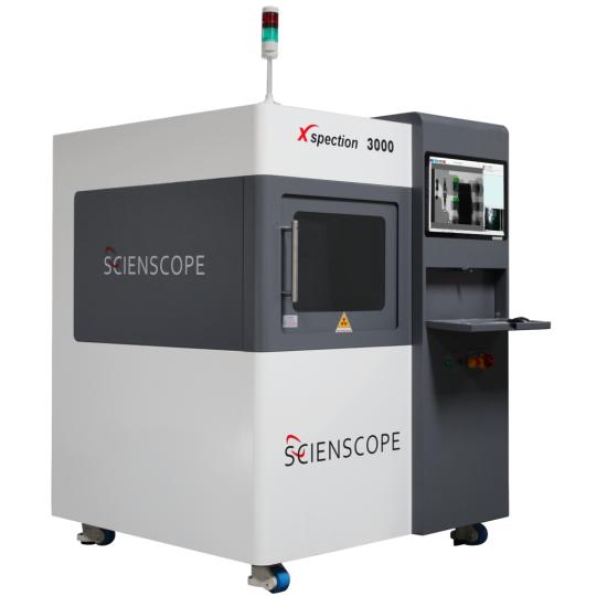
Scienscope - X-ray Inspection System Xspection 3000
IP-e50fe33d
Machine for offline X-Ray Inspection
Scienscope - X-ray Inspection System Xspection 3000
IP-e50fe33d
Machine for offline X-Ray Inspection
Besoin d'assistance, d'installation et/ou de formation ?
Appelez-nous +32 (0)14 42 44 01 ou contactez nous
Description
The Xspection 3000 is a single-closed tube, single flat panel detector, and all-purpose high-resolution X-Ray machine intended to perform both circuit board defect detection and quality insurance for the SMT industry worldwide. The X-ray machine has two main variants: the conventional 100kV version and the top-of-the-line 130kV version.
Highlights
- The new Al technology incorporates an advanced self-learning algorithm that can distinguish between bad and good images. lt adapts to the data it receives and continually improves its ability to identify and categorize images accurately.
- The enhanced TH barrel fill tool is designed to effectively identify and address voids that may occur during the through-hole filling process. By doing so, the improved tool aims to enhance the overall quality and reliability of the final product.
- Two high-resolution color cameras (20 Megapixel each) improve the mapping accuracy and make possible barcode reading and optical inspection upgrades.
Features
- Fully integrated 100kV or 130kV microfocus sealed tube
- Spot size down to 5 µm
- Larger flat panel detector increases field of view
- Added one more mapping camera for close-up image capture
- Self-learning Al software makes programming easy
- XV table has been upgraded to servo driven for a faster cycle
- Optional 360-degree rotating stage is lighter and taster
- Accurate VOID calculation by better background definition
- Enhanced BGA tool reduces false alarms
- lndustrial PC: Microsoft Windows 11
X-ray inspection: why so important?
1. Detection of Hidden Defects
Many defects in SMT components and PCBs (Printed Circuit Boards) are not visible to the naked eye or with traditional inspection methods. X-ray inspection allows for the detection of defects that are hidden beneath the surface, such as:
- Solder joints under components: Especially for BGAs (Ball Grid Arrays), where the solder connections are completely hidden underneath the component.
- Internal voids or delamination within PCB layers.
- Poor solder joints, such as cold solder joints or insufficiently melted solder, which can cause electrical failures.
2. Quality Control of Solder Joints
The quality of solder joints is critical to the reliability of electronic devices. X-ray inspection helps evaluate:
- Voids (air pockets) in solder joints: Voids can weaken the mechanical and electrical properties of a solder joint.
- Solder balling: Tiny balls of solder that may cause short circuits.
- Bridging: Unintended solder bridges between pads that can result in shorts.
- Excess or insufficient solder deposition, which can compromise the integrity of the connections.
3. Reliability and Longevity
Defects that go undetected can lead to early failure of electronic devices, especially in demanding environments (e.g., medical, aerospace, or automotive industries). X-ray inspection helps detect potential issues early in the production process, improving the reliability and longevity of the final product.
4. Non-Destructive Testing
A significant advantage of X-ray inspection is that it is a non-destructive test. This means that components or PCBs are not damaged during the inspection process. As a result, inspection can be carried out on fully assembled products without disassembling or damaging them.
5. Process and Production Optimization
By identifying defects, manufacturers can optimize and adjust their production processes to prevent future errors. This leads to higher production efficiency and fewer rejected products.
6. Suitability for High-Density Circuits
SMT components are often used in high-density PCBs, where space is limited and error margins are minimal. X-ray inspection enables detailed analysis of these complex structures, which might be difficult or impossible with other inspection methods.
Specifications
Maximum X and Y | 650mm x 500mm |
Maximum tilt | 45° (Optional 70°) |
Inspection speed | Servo XY |
Maximum X-Ray power | 100kV 5µm |
X-Ray flat panel detector | +/- 127 x 127 mm - 16bit |
Resolution | 1536px x 1536px |
Pixel size | 85µm |
360° rotating table | Optional |
Optical inspection camera | 2 x 20 Megapixels |
Automatic programing | Yes |
Fiducial recognition | Yes |
Automatic void percentage calculation | Yes |
BGA measuring | Yes |
Barcode | Optional (Optical optional camera) |
Offline programming | Optional |
Repair station | Optional |
SPC | Yes |
Windows 11 ready | Yes |
Dimensions (LxWxH) | 1510 x 1510 x 1870 mm, with tower light (2220mm) |
Weight | 1550 kg |
Electric | AC 110-240V VAC 50/60Hz |
The Xspection 3000 is a single-closed tube, single flat panel detector, and all-purpose high-resolution X-Ray machine intended to perform both circuit board defect detection and quality insurance for the SMT industry worldwide. The X-ray machine has two main variants: the conventional 100kV version and the top-of-the-line 130kV version.
Highlights
- The new Al technology incorporates an advanced self-learning algorithm that can distinguish between bad and good images. lt adapts to the data it receives and continually improves its ability to identify and categorize images accurately.
- The enhanced TH barrel fill tool is designed to effectively identify and address voids that may occur during the through-hole filling process. By doing so, the improved tool aims to enhance the overall quality and reliability of the final product.
- Two high-resolution color cameras (20 Megapixel each) improve the mapping accuracy and make possible barcode reading and optical inspection upgrades.
Features
- Fully integrated 100kV or 130kV microfocus sealed tube
- Spot size down to 5 µm
- Larger flat panel detector increases field of view
- Added one more mapping camera for close-up image capture
- Self-learning Al software makes programming easy
- XV table has been upgraded to servo driven for a faster cycle
- Optional 360-degree rotating stage is lighter and taster
- Accurate VOID calculation by better background definition
- Enhanced BGA tool reduces false alarms
- lndustrial PC: Microsoft Windows 11
X-ray inspection: why so important?
1. Detection of Hidden Defects
Many defects in SMT components and PCBs (Printed Circuit Boards) are not visible to the naked eye or with traditional inspection methods. X-ray inspection allows for the detection of defects that are hidden beneath the surface, such as:
- Solder joints under components: Especially for BGAs (Ball Grid Arrays), where the solder connections are completely hidden underneath the component.
- Internal voids or delamination within PCB layers.
- Poor solder joints, such as cold solder joints or insufficiently melted solder, which can cause electrical failures.
2. Quality Control of Solder Joints
The quality of solder joints is critical to the reliability of electronic devices. X-ray inspection helps evaluate:
- Voids (air pockets) in solder joints: Voids can weaken the mechanical and electrical properties of a solder joint.
- Solder balling: Tiny balls of solder that may cause short circuits.
- Bridging: Unintended solder bridges between pads that can result in shorts.
- Excess or insufficient solder deposition, which can compromise the integrity of the connections.
3. Reliability and Longevity
Defects that go undetected can lead to early failure of electronic devices, especially in demanding environments (e.g., medical, aerospace, or automotive industries). X-ray inspection helps detect potential issues early in the production process, improving the reliability and longevity of the final product.
4. Non-Destructive Testing
A significant advantage of X-ray inspection is that it is a non-destructive test. This means that components or PCBs are not damaged during the inspection process. As a result, inspection can be carried out on fully assembled products without disassembling or damaging them.
5. Process and Production Optimization
By identifying defects, manufacturers can optimize and adjust their production processes to prevent future errors. This leads to higher production efficiency and fewer rejected products.
6. Suitability for High-Density Circuits
SMT components are often used in high-density PCBs, where space is limited and error margins are minimal. X-ray inspection enables detailed analysis of these complex structures, which might be difficult or impossible with other inspection methods.