Pin-to-hole ratio in THT soldering: what is the ideal ratio?
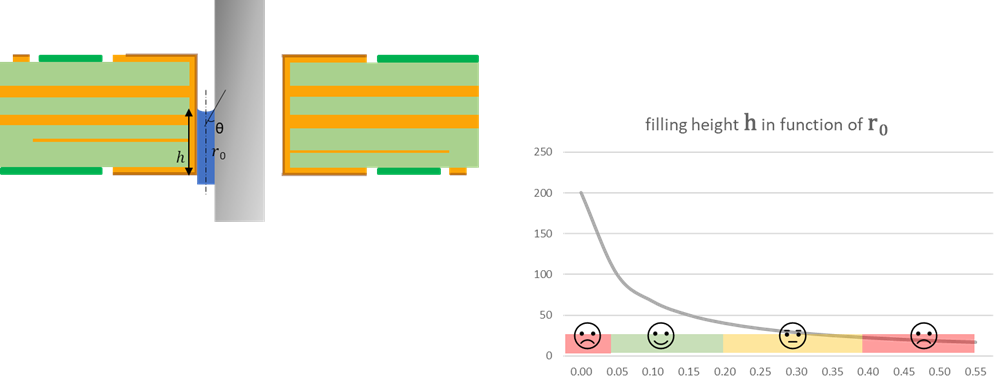
With THT components, good hole fill is important for creating a reliable solder joint. The ratio between the diameter of the component lead and the plated through-hole plays an important role. If the clearance is too large or too small, capillary action can be reduced, making it more difficult for molten solder to rise through the hole.
As a practical guideline, make the hole diameter approximately 0.5 mm larger than the diameter of the component lead. This creates around 0.25 mm of clearance on each side of the lead, providing favourable conditions for capillary action. However, the pin-to-hole ratio is not the only factor that determines whether the hole is properly filled.
Why is good hole fill important?
During wave and selective soldering, molten solder comes into contact with the component lead and plated through-hole from the underside of the PCB. The solder then needs to rise through the space between the lead and the wall of the hole.
The required level of hole fill depends, among other things, on the applicable quality class and the requirements of the product. Applications requiring high reliability generally have stricter requirements. It therefore makes sense to optimise both PCB design and the soldering process for the best possible solder rise.
Capillary action draws solder upwards
The upward movement of molten solder is largely caused by capillary action. A liquid can rise through a narrow opening against the force of gravity.
This phenomenon is described by Jurin’s law. For the soldering process, four factors are particularly relevant:
- the surface tension of the molten solder
- the contact angle between the solder and the surface to be wetted
- the density of the solder
- the clearance between the component lead and the wall of the hole
The last factor in particular can already be influenced during PCB design.
What is the ideal pin-to-hole ratio?
For THT soldering, a practical range for the clearance between the lead and the hole is approximately 0.1 to 0.4 mm per side. At around 0.25 mm per side, conditions are favourable for capillary action.
This results in a simple design guideline:
hole diameter = lead diameter + approximately 0.5 mm
For example, if a component has a lead diameter of 1.0 mm, a hole diameter of approximately 1.5 mm is a logical starting point from the perspective of capillary action.
A larger hole is therefore not automatically better. As the clearance increases, capillary action decreases. An extremely small clearance is not desirable either, as physical obstruction and resistance can restrict the flow of solder.
What other factors influence hole fill?
A correct pin-to-hole ratio does not guarantee complete hole fill. Several process parameters also play an important role.
Flux and wetting
For effective capillary action, the molten solder must properly wet the metal surfaces. Oxidation interferes with this process. Flux cleans and activates the surfaces, helping to reduce the contact angle.
It is therefore not only important to apply sufficient flux. The flux must also penetrate the hole before soldering takes place.
Nitrogen
Soldering in a nitrogen atmosphere reduces oxidation and influences the conditions under which molten solder wets the surfaces and rises through the hole. Nitrogen can therefore contribute to improved hole fill in both selective and wave soldering.
Temperature and thermal mass
Good geometry will not solve the problem if the solder cools down too much while rising through the hole. Once the solder solidifies, its upward movement stops.
This is particularly important with thicker multilayer PCBs and connections involving large amounts of copper. Copper dissipates heat quickly, which may require additional preheating or thermal relief in the PCB design.
Pump pressure
In wave and selective soldering, pump pressure helps force molten solder upwards. However, increasing the pressure cannot simply compensate for poor wetting or an unfavourable pin-to-hole ratio. The conditions required for capillary action still need to be present.
What if the hole fill is insufficient?
If solder does not rise sufficiently through the hole, do not focus solely on the soldering machine. Check the combination of lead diameter, hole diameter, flux penetration, wetting, temperature, thermal mass and process settings.
The guideline of approximately 0.25 mm clearance per side provides a useful starting point. For persistent problems, the complete thermal and soldering process should be evaluated. This prevents trying to solve a PCB design issue through process settings, or vice versa.
Conclusion
For strong capillary action in THT soldering, a hole diameter approximately 0.5 mm larger than the lead diameter is a practical guideline. Final hole fill, however, depends on the interaction between PCB design, wetting, flux, temperature, thermal mass and the soldering process.
Related trainings