Saki - In-line automated 3D X-ray inspection system 3Xi-M200
SAKI-X2
Inline 3D X-ray Inspection Machine for Power Module
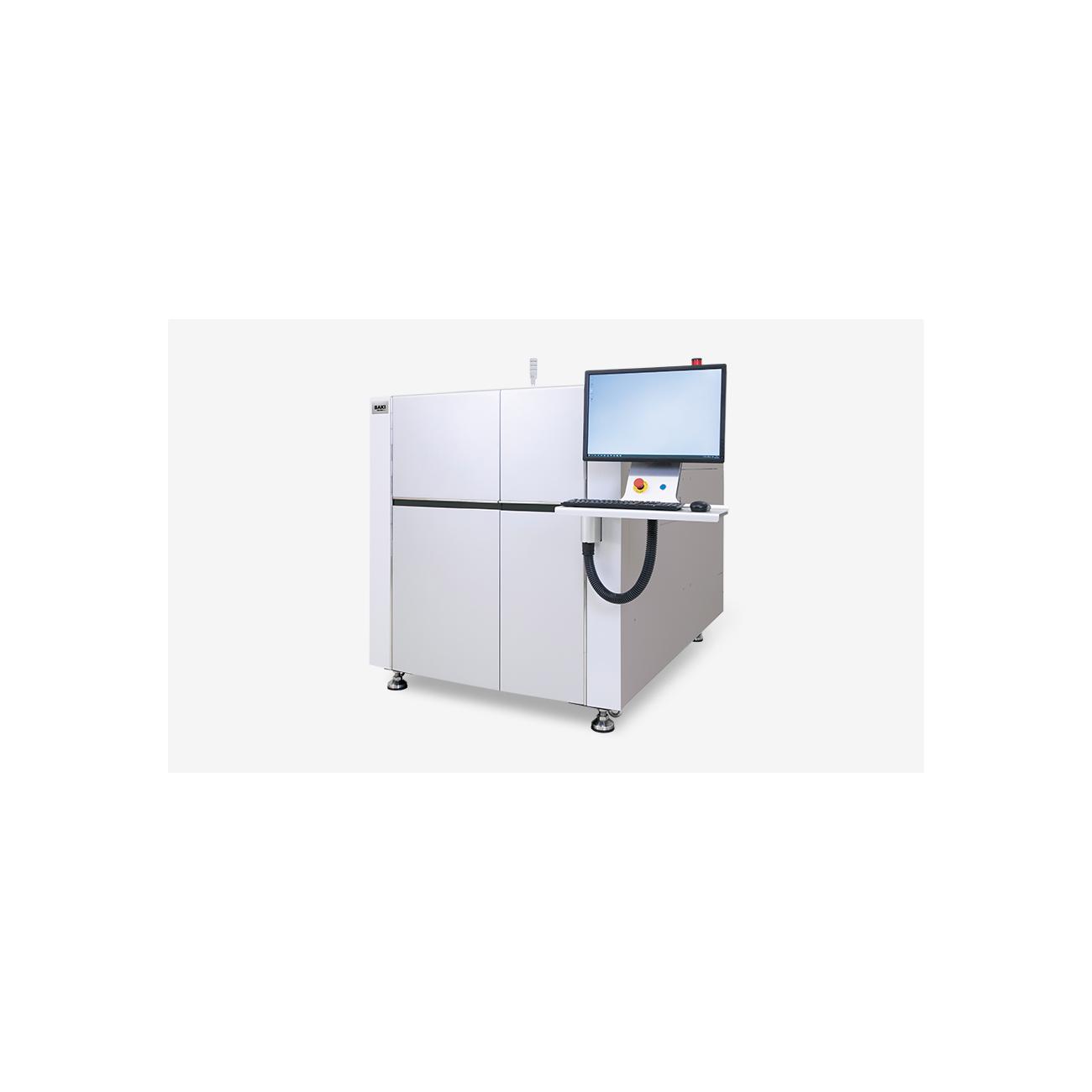
Saki - In-line automated 3D X-ray inspection system 3Xi-M200
SAKI-X2
Inline 3D X-ray Inspection Machine for Power Module
Contact us
Need a quote, installation, or training?
Call +32 (0)14 42 44 01 or contact us

Nick Janssen
Product specialist

Description
A high-speed, high-precision 3D-CT X-ray inspection system, compatible with SMT, through-hole processes and Semiconductor inspection process, SAKI’s 3D CT-AXI boasts the industry’s fastest speed, utlilizing superior 3D imaging and inspection quality to detect the full spectrum of solder defects on PCBs.
Our 3D-CT AXI include high-definition models and high-power, high-speed models to meet a variety of inspection requirements.
Powerful High-Speed, High-Definition Imaging
- The industry’s fastest imaging and calculation processing capability
- Detailed and true 3D image generation for zero-defect production
- Supports inspection of Slim and lightweight DSC power module
Ease of Use and Reduced Workload
- Easy-to-program automatic imaging condition settings can be taken from AOI
- Debugging can be undertaken without stopping the production line
Improved Maintainability and Ease of Maintenance
- Long-life hardware design for consistently high accuracy
- Self-diagnostic function, with exposure dose prediction and reduction
Specifications
| Size (WxDxH) | 1380 x 2150 x 1862 mm |
| Weight approx. | 5200 Kg |
| Electric power requirement | Single-phase ~ 200-240V +/-10%, 50/60Hz |
| Resolution | 51μm - 104μm |
| Tube | 180kV 90W, Closed X-ray Tube |
| X-ray leakage | 0.5μSv/h or less |
| Air requirement | 0.5MPa, 5 l/min (ANR) |
| Target board size in mm | 50 W x 140 L / 460 W x 440 L - 50 W x 140 L / 460 W x 600 L |
| PCB clearance | Top 68mm, Bottom 40mm |
A high-speed, high-precision 3D-CT X-ray inspection system, compatible with SMT, through-hole processes and Semiconductor inspection process, SAKI’s 3D CT-AXI boasts the industry’s fastest speed, utlilizing superior 3D imaging and inspection quality to detect the full spectrum of solder defects on PCBs.
Our 3D-CT AXI include high-definition models and high-power, high-speed models to meet a variety of inspection requirements.
Powerful High-Speed, High-Definition Imaging
- The industry’s fastest imaging and calculation processing capability
- Detailed and true 3D image generation for zero-defect production
- Supports inspection of Slim and lightweight DSC power module
Ease of Use and Reduced Workload
- Easy-to-program automatic imaging condition settings can be taken from AOI
- Debugging can be undertaken without stopping the production line
Improved Maintainability and Ease of Maintenance
- Long-life hardware design for consistently high accuracy
- Self-diagnostic function, with exposure dose prediction and reduction
| Size (WxDxH) | 1380 x 2150 x 1862 mm |
| Weight approx. | 5200 Kg |
| Electric power requirement | Single-phase ~ 200-240V +/-10%, 50/60Hz |
| Resolution | 51μm - 104μm |
| Tube | 180kV 90W, Closed X-ray Tube |
| X-ray leakage | 0.5μSv/h or less |
| Air requirement | 0.5MPa, 5 l/min (ANR) |
| Target board size in mm | 50 W x 140 L / 460 W x 440 L - 50 W x 140 L / 460 W x 600 L |
| PCB clearance | Top 68mm, Bottom 40mm |


