Why Step Stencils are indispensable in your PCB assembly

Miniaturization of electronic devices and components is a real trend. Designers are constantly working on the edge of the physical limits of manufacturability. As a result of this the apertures in stencils are always getting smaller. Who still remembers the times that a chip component of 2 by 3mm was really small? Nowadays components of 0,2 by 0,4mm are no exception!
As soon as the design is made and the PCB’s and components are purchased, assembling all the parts on a production line is the next mayor step. In this step stencils play a very important role.
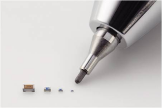
Miniaturisation of PCB components over the years.
Traditional stencils vs. Step Stencils
The common traditional stencils have a certain thickness along their entire surface. Because of miniaturization an increasing need for stencils with areas of lesser or more thickness has grown.
These type of stencils are called stepped stencils.
The minimum dimensions of the stencil apertures are depending on the stencil thickness. Smaller apertures require thinner stencils. As a result the choice of solder paste has to be reviewed.
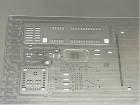
Example of Step Stencil
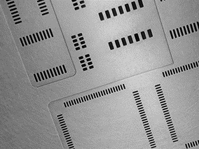
–
The importance of a solder paste
Solder paste is a mixture of fine grain solder powder and a gel flux. A solder paste is continuously subject to evolution. The grain size of the solder paste determines the filling of the apertures. The thinner a stencil, the better the release of paste from the stencil and the better the transfer of paste to the PCB will be.
Two decennia ago the standard powder in solder paste had a grain between 25 – 45 µm, nowadays the grain size has dropped to 15 -25µm.
The current solder paste machines have to be able to print complex electronic boards with a repeatable accuracy and very high precision. A robust, stable and high technological machine design is crucial in this process.
To excel in PCB assembly with the ESE stencil printer
The US-X series of stencil printers of the renown South Korean brand ESE has it all to fulfil and even surpass the highest production requirements.
The hart of the machine is their unique and robust printing table which has 4 ball screws along with 3LM guides. This design is unique and crucial and enables stable print accuracy of within 10µm and these are combined with a 12,5µm repeatability.
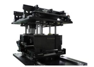
ESE’s robust, accurate and unique design print table
ESE’s US-X series is a very comprehensive machine with some very interesting features:
- Very intuitive software interface
- 2D inspection
- Under stencil cleaner,
- Automatic support pin placer,
- Solder paste high check,
- SPI feedback,
- Seamless board clamping,
- Internal climatisation
- Fast camera
Feedback of SPI data
An Solder Paste Inspection system (SPI) is an essential part of an SMD assembly line. An SPI system measures the shape, volume, the coverage and the positioning of the printed solder paste on the PCB. When these measurements are out of tolerance the SPI will report this and will send this data to the ESE printer.
The SPI can report clogged apertures to the ESE printer which will activate an additional cleaning cycle of the under stencil cleaner. Also the alignment in the printer can be corrected.
A leading manufacturer of automatic optical inspection systems for the electronic industry is the SAKI corporation. Their 3D solder paste inspection system inspects the whole surface of a PCB very accurately and fast.
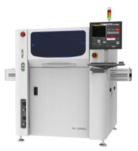
ESE Stencil Printer US-X-Series
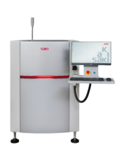
SAKI 3D Solder Paste Inspection (SPI)
The combination of the ESE printer and SAKI SPI ensures very reliable production of semi conductors and electronic PCB’s
Would you like more info?
Feel free to get in touch!
More info?
Please contact:
Bart van de Lisdonk
Service & Process Expert
0032 14 47 19 83
or
Leave your details via the contact form and we will contact you as soon as possible!


